

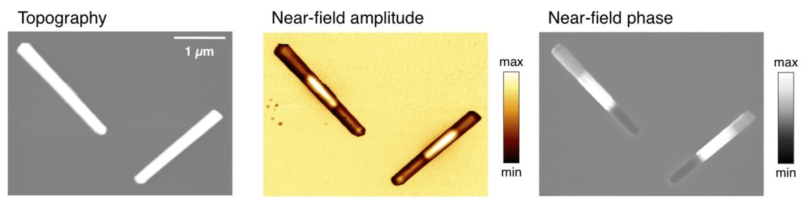
Near-field images of modulation doped InP nanowires yield pronounced contrasts between the differently doped segments. The topography image shows two, approx. 2µm long wires with a diameter of about 100nm. In the near-field amplitude (color) and phase (gray) image the individual segments can be clearly identified. Comparison of the near-field signals of the segments with model calculations even enables the quantification of the free carrier concentration. A gradient in the free carrier concentration between two adjacent segments can be investigated in detail and spatially mapped, yielding a spatial extension for the gradient of approx. 200nm.
The results demonstrate the application of infrared near-field microscopy for highly sensitive and nanoscale resolved mapping of free carriers in doped semiconductor nanowires.