

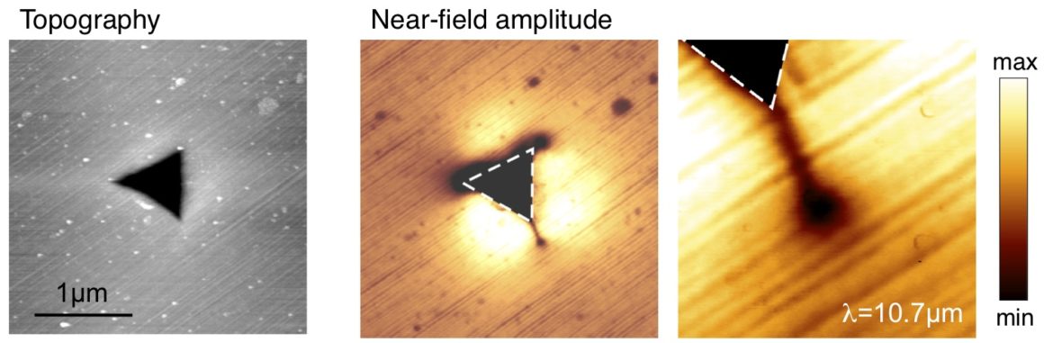
The high sensitivity of the near-field resonance of infrared-active materials to the structural properties allows to detect and spatially map local stress/strain fields on the surface by infrared near-field microscopy. To locally modify the crystal structure of a Silicon Carbide sample a sharp diamond tip was pressed into the sample surface (indentation) leading to compressive and tensile stress/strain fields around the plastic deformation zone. The topography image (gray) reveals the approx. 50nm deep triangular depression in the sample surface. The infrared (wavelength = 10.7µm) near-field image (color) clearly exhibits pronounced contrast features around the depression. Bright contrast corresponds to sample areas where compressive stress/strain is present. Dark contrast corresponds to tensile stress/strain, which predominantly occurs at the edges of the indent. The observed stress/strain field is characteristic around such indents. A higher resolution near-field image even reveals a small, approx. 250nm long, dark line emanating from the lower corner of the indent. The dark line is a clear signature of the stress/strain field associated to a nanoscale crack in the crystal lattice.
Applications of technological interest for nanoscale resolved stress/strain field mapping by infrared near-field microscopy could be the detection of nanocracks before they reach critical dimensions, and the study of crack propagation. Infrared near-field microscopy even offers the possibility of mapping free-carrier properties such as density and mobility in strained semiconductors. By controlled straining of e.g. silicon, the properties of the free carriers can be designed, which is essential to further shrink and speed-up future semiconductor devices.