

Researchers at the University of Stuttgart utilized neaspec microscope for successful imaging of switching process in a potent display material at previously unattainable nanoscale resolution. This groundbreaking work published in Science Advances opens a door towards novel ultrahigh-resolution displays in the future.
Showing content in virtual (VR) and augmented reality (AR) requires high-contrast displays with high pixel density. Development of such display technology requires nanoscale optical imaging tools with spatial resolution beyond the possibilities of conventional microscopy.
The size of pixels in state-of-the-art switchable optical devices is intrinsically limited by the fabrication of micrometer-sized transistors and spatial light modulators. To further decrease their size, several approaches are currently under debate and investigated in research labs all over the world. One promising route can be found in the field of nanoplasmonics. Plasmonic — or metallic — nanoparticles typically have sizes of only several tens of nanometers and could serve as individual display pixels. The color appearance of such pixels is determined by the nanoparticle size. By making the particles from a phase-change materials that can change between metallic and dielectric states, the colored pixels can be switched on and off. Thus, one can realize switchable colored plasmonic pixels with nanometer size and high contrast — thanks to a large differences between metallic and dielectric response.
One promising phase-change material for this purpose is magnesium. The well-known metal can, under external stimulus, hydrogenate to a dielectric insulator, showing a strong optical contrast. This makes it an ideal candidate for active and switchable systems, such as plasmonic color displays, dynamic holography platforms, etc. However, utilization of magnesium in optical devices has so far been limited by poor switching speed and cyclability,
 University of Stuttgart / PI 4")
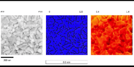
Measuring switching processes with previously unattainable ultrahigh nanoscale resolution
Researchers from the 4-th Physics Institute at the University of Stuttgart have succeeded for the first time to observe the switching process of this smart material with the much needed nanometer resolution, which is required to understand and analyze the influence of nanoscale morphology on the hydrogenation. In his experiment, Julian Karst from the group of Harald Giessen uses neaSCOPE microscope to image in-situ the changes in nanoscale optical and structural properties of free-standing magnesium. The measurements reveal an extreme influence of morphology on the nanoscale optical switching and provided insights for significant future performance improvements.
What is the future of phase-change materials?
“We are convinced that the published work will make a decisive contribution to the development of high-performance optical components with nanometer-sized pixels,” — emphasizes Prof. Harald Gießen. This could make visions such as 3D holographic VR glasses a reality in just a few years. Stuttgard researchers also sees further important implications of their work for the energy storage research, because magnesium is used as a hydrogen storage medium. Deeper understanding of diffusion processes on the nanometer scale could lead to a significant improvement of storage capacity and potentially bringing forward clean fuel cell technology.