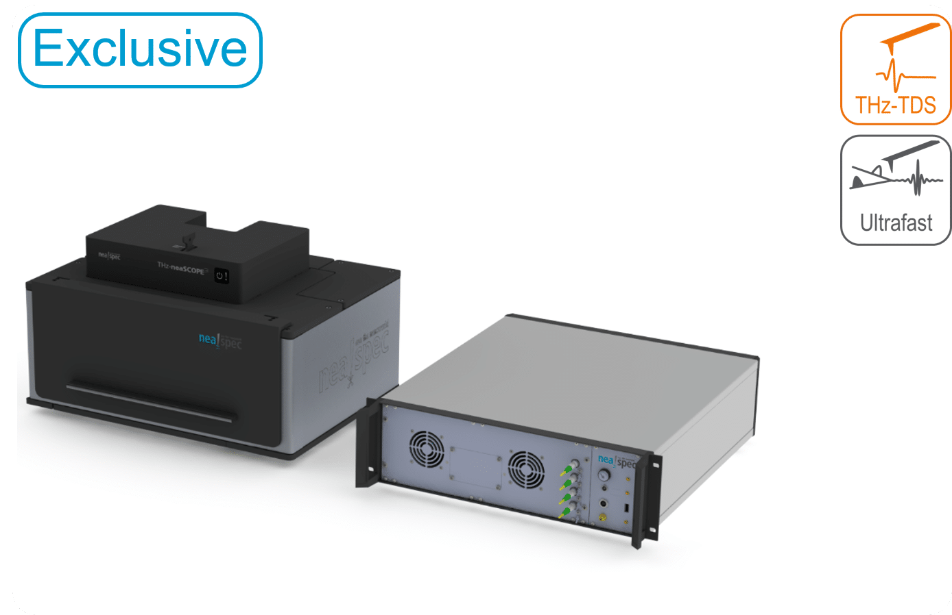
Due to their long wavelengths, terahertz radiation runs into difficulties when detecting extremely small structures. However, by combining terahertz radiation with a near-field microscope, it is possible to increase the lateral resolution into the nanometer range. neaspec developed a ready-to-use terahertz system that is capable of achieving a spatial resolution of 30 nanometers.

neaspec’s neaSCOPE near-field microscope for terahertz near-field measurements is opening up new possibilities in materials research
In comparison to visible light, terahertz radiation has a quite long wavelength of around 300 micrometers. This, unfortunately, limits the lateral resolution of terahertz measurements in the far-field zone to roughly 150 micrometers. A measurement accuracy of this proportion is often insufficient for materials research, where the analysis of the small-scale distribution of materials, for example in semiconductor components, requires spatial resolutions in the nanometer scale. Terahertz near-field measurements provide the solution to this conundrum.

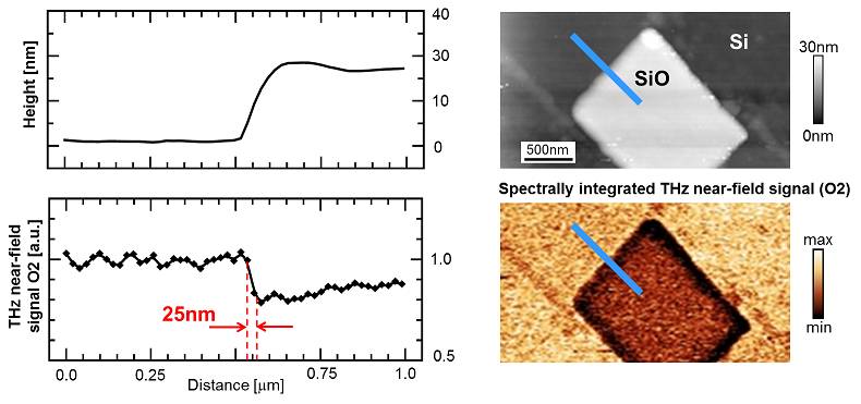
Images of semiconductor structures obtained by an atomic force microscope (above) and terahertz near-field microscope neaSCOPE (below). The images show an SiO structure of around 1.5 x 1 µm on an Si substrate (topography, grey). In the height profile, it can be observed that the structure has a thickness of around only 22 nm. Despite the thin layer of material, the terahertz near-field image (bottom right) recorded at the same time as the topography image provides a distinct contrast between the substrate and oxide. In addition to the extreme sensitivity of the terahertz near-field measurements when examining very thin layers, a line graph indicates the technology’s extraordinary spatial resolution (approximately 25–30 nm)
Terahertz near-field microscopy at resolutions below 30 nanometers
By combining terahertz radiation with a scattering-type near-field microscope, the natural resolution limit in the far-field zone is overcome. This opens up entirely new possibilities for conducting terahertz spectroscopy in materials research, such as during the quality control of industrially produced semiconductor components. At full spectral resolution in the terahertz region, the system developed was able to obtain images with a high degree of sensitivity to materials and a spatial resolution < 30 nm. This is less than a thousandth of the wavelength used.
In comparison to infrared measurements, the use of terahertz radiation increases sensitivity a hundredfold, for example when measuring the conductivity of semiconductor materials. Such an excellent rate of sensitivity is rarely achieved by other optical microscopy techniques. In fact, no other measuring method to date enables the qualitative mapping of material and charge carrier concentrations with nanoscale resolution. The ability to detect and quantify charge carriers opens up enormous potential for the use of terahertz near-field microscopy.
In fundamental physics research, the non-contact, non-invasive and quantitative mapping of mobile charge carriers with nanoscale resolution will provide crucial insights into unanswered questions in areas such as superconductors, low-dimensional conductors and correlated conductors.
In analytics, terahertz nanoscopy could become an interesting tool for the chemical and structural analysis of compounds and biological systems, as terahertz radiation is highly sensitive to the vibrations of crystal structures and molecules. Here, terahertz spectroscopy is particularly sensitive to structural changes in comparison to Raman and IR spectroscopy, allowing it to differentiate between various hydrate forms and isomers, for example.

