

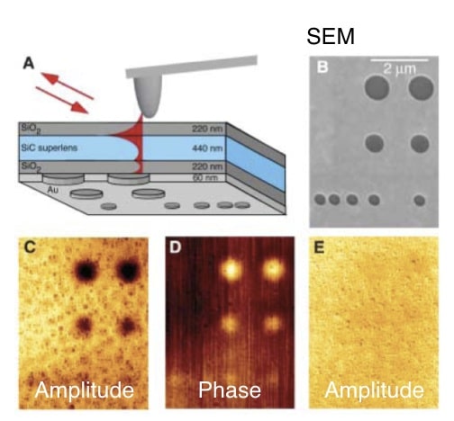
Near-field microscopy allows to investigate and to verify superlensing in amplitude and phase. For such a study a SiC superlens consisting of a 440nm thick SiC crystal sandwiched between two 220nm thick SiO2 layers was investigated. As imaged objects a patterned Au film evaporated on one side (bottom) of the lens with holes of different diameters was used. Infrared illumination and detection was performed through the lens from the same side (top) and the recorded near-field images demonstrate that a 540nm hole could be resolved by the superlens at a wavelength of about 11µm (approx 1/20 of the wavelength).
Possible applications include e.g the imaging of biological objects in their natural environment. Further, near-field microscopy studies of metameterials or negative refraction could provide further insight into the functionality of future photonic devices.