

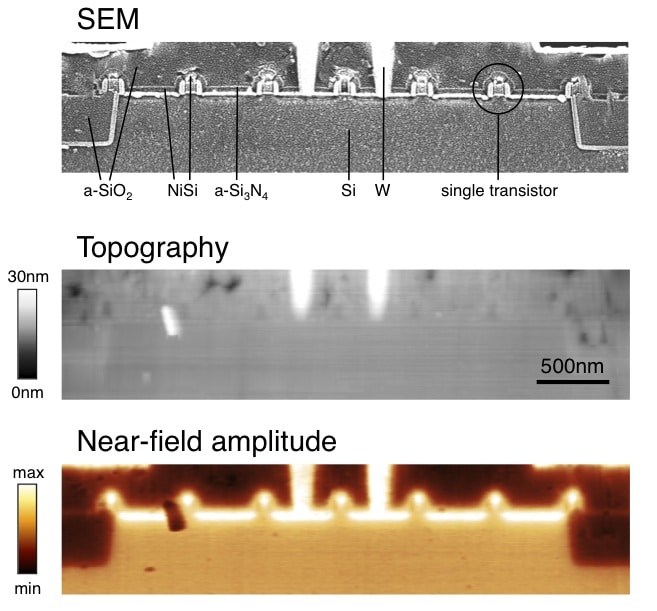
Infrared-active materials processed in semiconductor devices yield characteristic near-field spectral signatures allowing to identify the materials. A SEM image (gray) of a transistor test structure fabricated by the C65 technology node reveals the different materials and highlights the interface between them because of an applied decoration etch. Clearly, the seven individual transistors can be seen. The topography image of the cross sectional sample exhibits a flat surface as a result of the sample polishing process. The near-field amplitude image (color) reveals a high signal for metallic components, a medium signal for the Si substrate and a low signal for the insulating SiO.
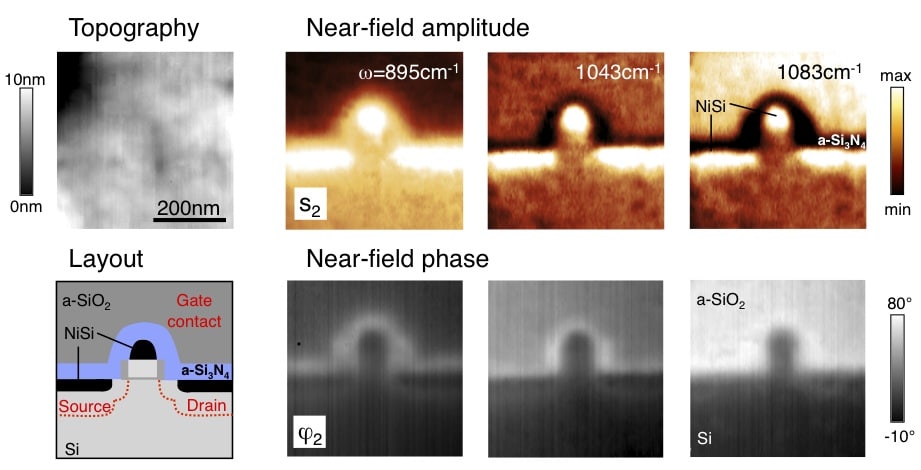
Recording a single transistor at higher resolution demonstrates the capabilities of neaSCOPE to analyze a single transistor. Depending on laser frequency used for near-field imaging the SiN or SiO components of the device can be highlighted. Compare near-field amplitude images (color) and device layout. The dependence of the contrasts on the frequency can be explained by material-specific near-field resonances, which enables the identification of the materials. The high sensitivity of near-field resonances to a materials dielectric properties allows to analyze the device components in detail.
Images taken in cooperation with Infineon Technologies, Munich (Dr. J. Wittborn).