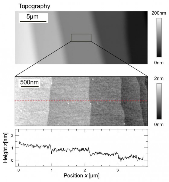
neaSNOM AFM topographic resolution with characteristic test structure
Sample details:
- Si echeloned test pattern (STEPP sample of NT-MDT)
- Surface exhibits larger terraces with step heights of approx. 30-50nm (upper image)
- Terraces contain single monoatomic steps with a height of 0.314nm (lower image)
- Specified average roughness of area without steps approx. 0.06nm
Results:
- Imaged at ambient conditions
- No signal analysis was applied, e.g. filtering (only line correction)
- Profile of single scan line (no averaging)
- Noise on flat area ≈0.027nm (RMS)
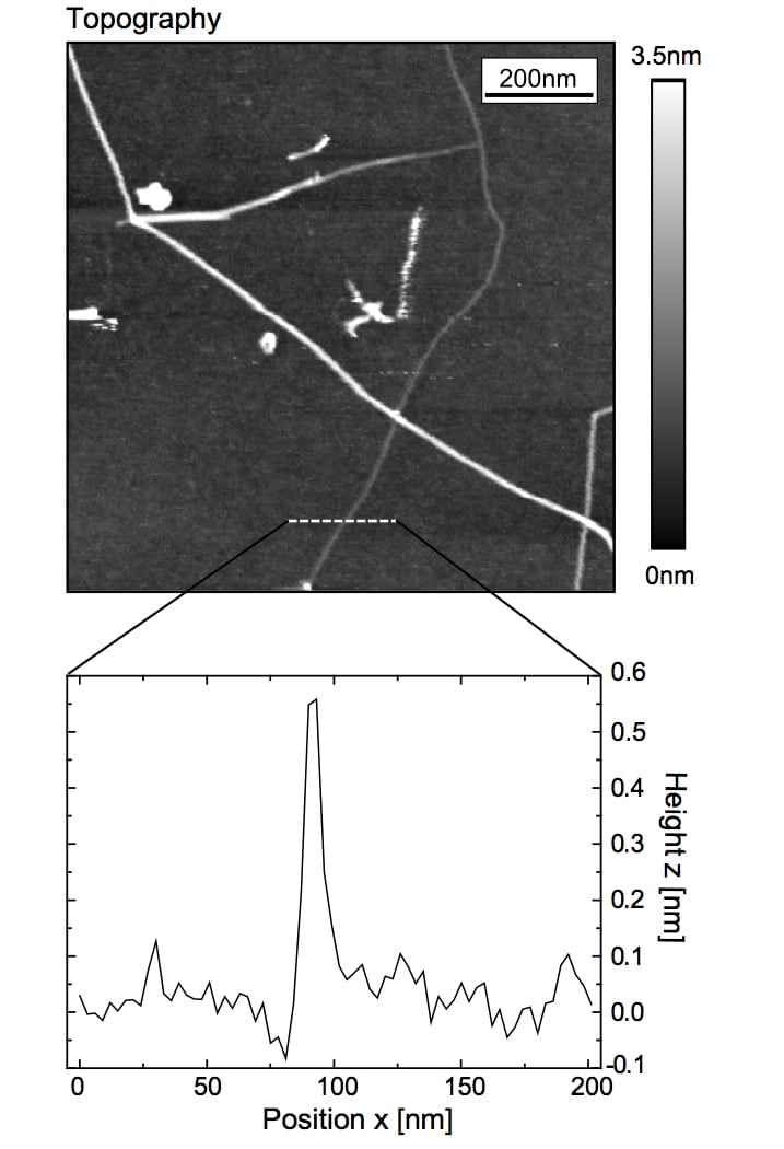
Topographic imaging of single-wall carbon nanotubes
Sample details:
- CVD grown single-walled carbon nanotubes (SWCNTs) spincast from dispersion on Si-substrate
- Silicon AFM tip (nominal tip radius ca. 10nm)
- Individual SWCNTs (nominal diameter <1nm)
- Bundles of SWCNTs (nominal diameter >3nm)
Scan details:
- Scan size 1×1µm, 333×333 pixel
- Scan speed 0.33s/line, 3Hz
Results:
- Imaged at ambient conditions
- No signal analysis was applied, e.g. filtering (only line correction)
- Profile of single scan line exhibits SWCNT height of <0.6nm


